- 您现在的位置:买卖IC网 > Sheet目录329 > IDT70T651S12DRI (IDT, Integrated Device Technology Inc)IC SRAM 9MBIT 12NS 208QFP
IDT70T651/9S
High-Speed 2.5V 256/128K x 36 Asynchronous Dual-Port Static RAM
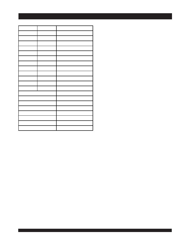
Pin Names
Industrial and Commercial Temperature Ranges
Left Port
CE 0L , CE 1L
R/ W L
OE L
Right Port
CE 0R , CE 1R
R/ W R
OE R
Names
Chip Enables (Input)
Read/Write Enable (Input)
Output Enable (Input)
A 0R - A 17R
A 0L - A 17L
(1)
(1)
Address (Input)
I/O 0L - I/O 35L
SEM L
INT L
BUSY L
BE 0L - BE 3L
V DDQL
OPT L
ZZ L
I/O 0R - I/O 35R
SEM R
INT R
BUSY R
BE 0R - BE 3R
V DDQR
OPT R
ZZ R
M/ S
Data Input/Output
Semaphore Enable (Input)
Interrupt Flag (Output)
Busy Flag (Output)
Byte Enables (9-bit bytes) (Input)
Power (I/O Bus) (3.3V or 2.5V) (2) (Input)
Option for selecting V DDQX (2,3) (Input)
Sleep Mode Pin (4) (Input)
Master or Slave Select (Input) (5)
V DD
V SS
TDI
TDO
TCK
TMS
TRST
Power (2.5V) (2) (Input)
Ground (0V) (Input)
Test Data Input
Test Data Output
Test Logic Clock (10MHz) (Input)
Test Mode Select (Input)
Reset (Initialize TAP Controller) (Input)
5632 tbl 01
6
NOTES:
1. Address A 17 x is a NC for IDT70T659.
2. V DD , OPT X , and V DDQX must be set to appropriate operating levels prior to
applying inputs on I/O X .
3. OPT X selects the operating voltage levels for the I/Os and controls on that port.
If OPT X is set to V DD (2.5V), then that port's I/Os and controls will operate at 3.3V
levels and V DDQX must be supplied at 3.3V. If OPT X is set to V SS (0V), then that
port's I/Os and controls will operate at 2.5V levels and V DDQX must be supplied
at 2.5V. The OPT pins are independent of one another—both ports can operate
at 3.3V levels, both can operate at 2.5V levels, or either can operate at 3.3V
with the other at 2.5V.
4. The sleep mode pin shuts off all dynamic inputs, except JTAG inputs, when
asserted. OPTx, INT x, M/ S and the sleep mode pins themselves (ZZx) are
not affected during sleep mode. It is recommended that boundry scan not be
operated during sleep mode.
5. BUSY is an input as a Slave (M/ S =V IL ) and an output when it is a Master
(M/ S =V IH ).
发布紧急采购,3分钟左右您将得到回复。
相关PDF资料
IDT70T653MS12BCI
IC SRAM 18MBIT 12NS 256BGA
IDT70V05L55G
IC SRAM 64KBIT 55NS 68PGA
IDT70V06L55G
IC SRAM 128KBIT 55NS 68PGA
IDT70V07L35G
IC SRAM 256KBIT 35NS 68PGA
IDT70V08S15PF
IC SRAM 512KBIT 15NS 100TQFP
IDT70V09L20PFI
IC SRAM 1MBIT 20NS 100TQFP
IDT70V18L20PFI
IC SRAM 576KBIT 20NS 100TQFP
IDT70V25L55G
IC SRAM 128KBIT 55NS 84PGA
相关代理商/技术参数
IDT70T651S15BC
功能描述:IC SRAM 9MBIT 15NS 256BGA RoHS:否 类别:集成电路 (IC) >> 存储器 系列:- 标准包装:3,000 系列:- 格式 - 存储器:EEPROMs - 串行 存储器类型:EEPROM 存储容量:8K (1K x 8) 速度:400kHz 接口:I²C,2 线串口 电源电压:1.7 V ~ 5.5 V 工作温度:-40°C ~ 85°C 封装/外壳:8-SOIC(0.154",3.90mm 宽) 供应商设备封装:8-SOIC 包装:带卷 (TR)
IDT70T651S15BC8
功能描述:IC SRAM 9MBIT 15NS 256BGA RoHS:否 类别:集成电路 (IC) >> 存储器 系列:- 标准包装:3,000 系列:- 格式 - 存储器:EEPROMs - 串行 存储器类型:EEPROM 存储容量:8K (1K x 8) 速度:400kHz 接口:I²C,2 线串口 电源电压:1.7 V ~ 5.5 V 工作温度:-40°C ~ 85°C 封装/外壳:8-SOIC(0.154",3.90mm 宽) 供应商设备封装:8-SOIC 包装:带卷 (TR)
IDT70T651S15BF
功能描述:IC SRAM 9MBIT 15NS 208FBGA RoHS:否 类别:集成电路 (IC) >> 存储器 系列:- 标准包装:3,000 系列:- 格式 - 存储器:EEPROMs - 串行 存储器类型:EEPROM 存储容量:8K (1K x 8) 速度:400kHz 接口:I²C,2 线串口 电源电压:1.7 V ~ 5.5 V 工作温度:-40°C ~ 85°C 封装/外壳:8-SOIC(0.154",3.90mm 宽) 供应商设备封装:8-SOIC 包装:带卷 (TR)
IDT70T651S15BF8
功能描述:IC SRAM 9MBIT 15NS 208FBGA RoHS:否 类别:集成电路 (IC) >> 存储器 系列:- 标准包装:3,000 系列:- 格式 - 存储器:EEPROMs - 串行 存储器类型:EEPROM 存储容量:8K (1K x 8) 速度:400kHz 接口:I²C,2 线串口 电源电压:1.7 V ~ 5.5 V 工作温度:-40°C ~ 85°C 封装/外壳:8-SOIC(0.154",3.90mm 宽) 供应商设备封装:8-SOIC 包装:带卷 (TR)
IDT70T651S15DR
功能描述:IC SRAM 9MBIT 15NS 208QFP RoHS:否 类别:集成电路 (IC) >> 存储器 系列:- 标准包装:3,000 系列:- 格式 - 存储器:EEPROMs - 串行 存储器类型:EEPROM 存储容量:8K (1K x 8) 速度:400kHz 接口:I²C,2 线串口 电源电压:1.7 V ~ 5.5 V 工作温度:-40°C ~ 85°C 封装/外壳:8-SOIC(0.154",3.90mm 宽) 供应商设备封装:8-SOIC 包装:带卷 (TR)
IDT70T651S8BC
功能描述:IC SRAM 9MBIT 8NS 256BGA RoHS:否 类别:集成电路 (IC) >> 存储器 系列:- 标准包装:3,000 系列:- 格式 - 存储器:EEPROMs - 串行 存储器类型:EEPROM 存储容量:8K (1K x 8) 速度:400kHz 接口:I²C,2 线串口 电源电压:1.7 V ~ 5.5 V 工作温度:-40°C ~ 85°C 封装/外壳:8-SOIC(0.154",3.90mm 宽) 供应商设备封装:8-SOIC 包装:带卷 (TR)
IDT70T651S8BC8
功能描述:IC SRAM 9MBIT 8NS 256BGA RoHS:否 类别:集成电路 (IC) >> 存储器 系列:- 标准包装:3,000 系列:- 格式 - 存储器:EEPROMs - 串行 存储器类型:EEPROM 存储容量:8K (1K x 8) 速度:400kHz 接口:I²C,2 线串口 电源电压:1.7 V ~ 5.5 V 工作温度:-40°C ~ 85°C 封装/外壳:8-SOIC(0.154",3.90mm 宽) 供应商设备封装:8-SOIC 包装:带卷 (TR)
IDT70T651S8BF
功能描述:IC SRAM 9MBIT 8NS 208FBGA RoHS:否 类别:集成电路 (IC) >> 存储器 系列:- 标准包装:3,000 系列:- 格式 - 存储器:EEPROMs - 串行 存储器类型:EEPROM 存储容量:8K (1K x 8) 速度:400kHz 接口:I²C,2 线串口 电源电压:1.7 V ~ 5.5 V 工作温度:-40°C ~ 85°C 封装/外壳:8-SOIC(0.154",3.90mm 宽) 供应商设备封装:8-SOIC 包装:带卷 (TR)
